Electromagnetic waves consist of two primary components: a magnetic field and an electric field. These fields are oriented perpendicularly to each other, and the direction in which the wave propagates is at a right angle to the plane formed by these two components. The relative strength of the magnetic (H) field and the electric (E) field depends on the distance from the wave’s source and the nature of the source itself. The ratio between the electric field (E) and magnetic field (H) is referred to as wave impedance, denoted as Zw.
If the source generates a large current relative to its voltage, such as in loops, transformers, or power lines, it is called a current, magnetic, or low impedance source. This classification stems from the small E-to-H ratio. On the other hand, when the source has a high voltage but low current, it is considered a high impedance source, and the wave is primarily associated with an electric field. At great distances from the source, the E-to-H ratio becomes the same for both types of waves, and the wave is referred to as a plane wave, with a wave impedance of 377 ohms, which is the intrinsic impedance of free space. Beyond this point, the curvature of the wave diminishes, and the field behaves as though it exists on a flat surface rather than on a spherical one, as with point sources.
Wave impedance plays a critical role when an electromagnetic wave encounters a discontinuity. If the wave impedance differs significantly from the intrinsic impedance of the material at the boundary, most of the wave energy will be reflected rather than transmitted. Most metals have an intrinsic impedance of only a few milliohms. For low impedance fields, where the magnetic field dominates, less energy is reflected and more is absorbed because the metal’s impedance is closer to the field’s impedance. This is why shielding against magnetic fields is particularly challenging. In contrast, electric fields, with their higher wave impedance, tend to reflect most of their energy upon encountering a discontinuity.
Consider the case of a wave striking a metallic surface at a right angle, as depicted in Figure 1. If the metal has infinite conductivity, the shield generates an electric field equal and opposite to the wave’s incident electric field, canceling out the tangential electric field at the boundary. In this ideal scenario, the shielding would be perfect, as the electric fields would completely cancel each other. Since the magnetic fields are in phase, the current within the shield doubles.
In reality, however, metallic enclosures do not provide perfect shielding, as the conductivity of metals is finite. Nonetheless, metals with high conductivity can still provide effective shielding. Due to their finite conductivity, part of the electromagnetic field penetrates the metal, inducing a current within the shield as shown in Figure 2. The amount of current at different depths and the rate of decay are determined by the metal’s conductivity and permeability. The remaining current on the far side of the shield generates the field on the opposite side.
 Figure 1
From Figures 2 and 3, we can conclude that thickness significantly impacts shielding performance. However, when skin depth is considered, thickness is only crucial at low frequencies. At higher frequencies, even thin metal foils can serve as effective shields.
Figure 3 illustrates the current density for thin shields, which is the same as for thick shields. In all cases, a secondary reflection occurs at the shield’s far side, regardless of its thickness. The key difference with thin shields is that a significant portion of the re-reflected wave may appear on the front surface. Depending on the phase relationship, this wave can either reinforce or cancel out the primary reflected wave. As a result, shielding calculations for thin shields include a correction factor to account for reflections from the far side of the shield.

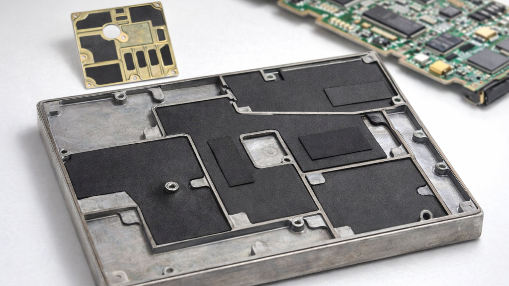
A gap or slot in a shield allows electromagnetic fields to pass through unless the continuity of current flow across the gap is maintained. The purpose of an EMI gasket is to ensure this continuity in the shield.
If the gasket material is identical to the shield’s walls, the current distribution in the gasket would ideally match that of the shield, assuming the gasket could completely fill the gap. However, this is not fully achievable due to mechanical limitations.
Figure 4 illustrates the current flow through a shield and its gasket interface. Electromagnetic leakage at the seam can occur in two ways. First, energy may pass directly through the gasket material. In Figure 4, the gasket has lower conductivity than the shield material, leading to a slower rate of current decay in the gasket. Consequently, more current reaches the far side of the shield, increasing the leakage field.
Second, leakage can occur at the interface between the gasket and the shield. If an air gap is present in the seam, the current is forced to flow through the points of contact, causing changes in the current distribution in both the shield and the gasket. A high-resistance joint behaves similarly to open seams, only slightly modifying the current distribution. Figure 4 shows a typical current distribution in a seam, where wider spacing between lines of constant current indicates reduced current flow. To minimize leakage, it is important to design gaskets with electrical properties as similar to the shield as possible, maintain high conductivity at the interface, and eliminate air gaps or high-resistance areas.

Shielding and Gasket Equations
The previous section provided a physical understanding of the core principles behind shielding and gasketing. In this section, we focus on the mathematical expressions useful for general design purposes, helping to establish criteria for selecting parameters in a shielded enclosure.
As discussed earlier, when electromagnetic waves encounter a discontinuity, part of the wave is reflected while the rest is transmitted across the boundary and into the material. The overall effectiveness of the shield combines these two effects, along with a correction factor to account for reflections from the back surface of the shield. The general equation for shielding effectiveness is expressed as:
SE = R + A + B (1)
Where:
- SE represents shielding effectiveness
- R is the reflection factor
- A is the absorption factor
- B is the correction factor for reflections from the far boundary
The reflection term depends primarily on the mismatch between the incoming wave and the shield’s surface impedance. The reflection terms for different types of waves have been derived by others, and the equations for the three principal field types are as follows:

Polarization Effects
The currents induced in a shield flow in the same direction as the electric field component of the incoming wave. For instance, if the electric field component is vertical, the wave is considered vertically polarized, and it will generate a vertically flowing current in the shield.
A gasket placed perpendicular to the current flow is less effective than one aligned parallel to it.
A circularly polarized wave contains equal vertical and horizontal components, meaning gaskets must provide equal effectiveness in both directions. When polarization is unknown, gasketed junctions should be designed and tested under the worst-case scenario, where the current flows parallel to the gasket seam.
Nomographs
The nomographs in Figures 6 through 9 assist designers in determining absorption and magnetic field reflection losses directly. These nomographs are derived from the equations discussed earlier.
Absorption Loss – Figure 6:
To find the required thickness for a given metal to achieve a specific absorption loss at a known frequency:
a. Find the frequency on the “f” scale and the desired absorption loss on the “A” scale. Place a straightedge between these points and mark the intersection on the unmarked “X” scale (e.g., A = 10 dB, f = 100 kHz).
b. Pivot the straightedge across the “G x μ” scale for different metals to determine the necessary thickness on the “t” scale (e.g., for copper, t = 9.5 mils; for cold rolled steel, t = 2.1 mils). Be cautious when using these charts for ferrous materials, as permeability (μ) varies with magnetizing force.
Magnetic Field Reflection – Figure 7:
To determine magnetic field reflection loss (RH):
a. Identify the point on the “G/μ” scale for the desired metal. For unlisted metals, calculate G/μ and find the corresponding point on the numerical scale.
b. Find the distance between the energy source and the shield on the “r” scale.
c. Draw a line between “r” and “G/μ” to locate a point on the unmarked “X” scale (e.g., r = 10 inches for hot rolled steel).
d. Connect this point on the “X” scale with the desired frequency on the “f” scale.
e. Read the reflection loss on the “RH” scale (e.g., for f = 10 kHz, RH = 13 dB).
f. To plot RH versus frequency, move along the “f” scale while keeping the point on the “X” scale fixed (e.g., for f = 1 kHz, RH = 3.5 dB). Note that thickness does not affect reflection loss calculations.
Magnetic Field Secondary Reflection Losses (|K|) – Figures 8 and 9:
To determine the secondary magnetic field reflection loss factor (|K|) and solve for B:
Given: r = 2 inches, t = 0.0162 in. thick copper, and A = 1.3 dB. Find B at 1 kHz.
a. Draw a line between copper on the “G/μ” scale and r = 2 inches on the “source to shield distance” scale to locate a point on the “X” scale.
b. Draw another line from the “X” scale to 1 kHz on the “f” scale.
c. At the intersection with the “|K|” scale, read |K| = 2.2 x 10⁻².
d. Move to Figure 9.
e. In Figure 9, locate |K| = 2.2 x 10⁻² on the horizontal scale.
f. Move vertically to the A = 1.3 curve (interpolating if necessary), then horizontally to find B = –8.5 dB.
Electromagnetic Compatibility and Interference
Electromagnetic compatibility (EMC) occurs when electronic devices operate as intended in their environment without emitting or being susceptible to excessive electromagnetic energy from internal or external sources. Electromagnetic interference (EMI) is unwanted radiated or conducted energy that disrupts a device’s EMC, adversely affecting circuit performance. Many electronic circuits either emit or are vulnerable to EMI, requiring shielding for proper operation.
Establishing EMC in electronic devices typically involves two strategies. The first is minimizing internally generated EMI, as shown in Figure 1, which can be achieved by designing circuits to inherently generate less EMI. Any remaining EMI can then be suppressed or contained within the enclosure using appropriate shielding and filtering techniques. Filtering cables where they enter or exit the enclosure reduces conducted emissions.
Matrix specializes in customization to meet the exact specifications required by manufacturers. Our state-of-the-art equipment and expertise ensure precise detail, providing manufacturers with tailored solutions to enhance their product quality and performance.


